
Hole Mobility vs Electron Mobility: How Much Slower Is a PMOS Than an NMOS in Sub-Micron Silicon
Ever wondered why microprocessors were historically designed with massive, oversized p-channel transistors just to keep up with their n-channel siblings? If you have spent any time laying out custom CMOS logic or analyzing timing paths in modern integrated circuits, you have undoubtedly bumped into this pesky physics problem. The battle of hole mobility vs electron mobility is one of the foundational trade-offs in semiconductor engineering.
Here is the short answer: historically, a PMOS device was anywhere from 2 to 3 times slower than an NMOS device of identical physical dimensions. But once we shrunk gate lengths down into the sub-micron and nanometer regimes, that gap shrank considerably due to high-field velocity saturation and aggressive strain engineering. Look—physics didn't change, but our clever trickery with silicon crystals certainly did.
Honestly? Understanding this gap is not just academic trivia. It dictates how we size logic gates, manage parasitic capacitance, balance propagation delays, and optimize modern high-speed designs.
Let's dive deep into the silicon lattice to see why electrons zip around while holes lag behind, how sub-micron short-channel effects alter the math, and what chip designers do to level the playing field.
The Physics Behind Carrier Velocity: Why Electrons Leave Holes in the Dust
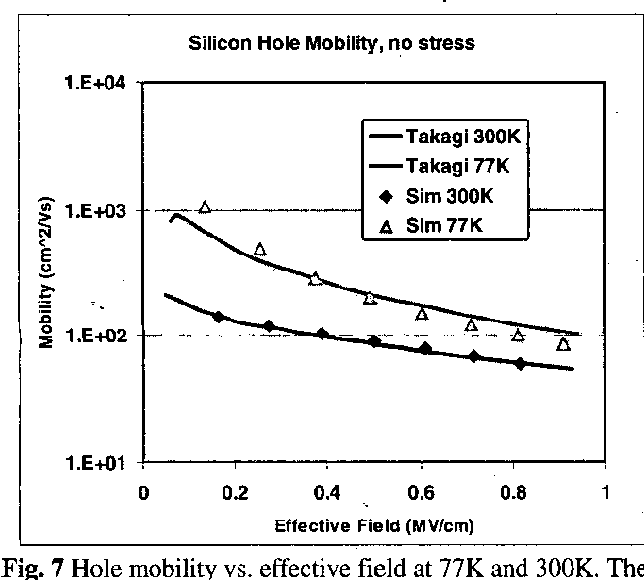
To understand why a PMOS transistor feels like it's wearing concrete shoes compared to an NMOS, we have to look directly at quantum mechanics and crystal structure. In intrinsic silicon at room temperature, electron mobility sits around 1350 cm²/V·s, while hole mobility drags behind at roughly 480 cm²/V·s. That is a massive fundamental disparity right off the bat.
Why such a huge difference? It comes down to how charge carriers actually travel through a semiconductor crystal. An electron in the conduction band moves almost like a free particle in a periodic potential, bouncing off crystal lattice vibrations with relatively light resistance. A hole, on the other hand, isn't a physical particle at all—it is an empty quantum state in the valence band, requiring adjacent electrons to sequentially jump into vacant spots to create movement.
Think of it like a crowded parking lot. An electron is a motorcycle weaving through open space. A hole is an empty parking space moving backward because cars are sequentially pulling into it one by one. Which process takes more effort? Exactly.
Furthermore, the energy band structure of silicon dictates the underlying effective mass of these carriers. Lower effective mass translates directly to higher acceleration under an applied electric field, which brings us to the core equations governing carrier motion.
Effective Mass and Energy Band Structures
In solid-state physics, a carrier's mobility ($\mu$) is inversely proportional to its effective mass ($m^$) and directly proportional to its mean free time between scattering events ($\tau$). The classic equation $\mu = q\tau / m^$ tells the whole story. Electrons in the silicon conduction band occupy six equivalent energy valleys, yielding a relatively light conductivity effective mass of about 0.26 $m_0$ (where $m_0$ is the rest mass of a free electron).
Holes reside in the valence band, which is far more complex. The valence band consists of heavy-hole, light-hole, and split-off sub-bands. Because the heavy-hole band dominates the density of states at room temperature, the average effective mass for holes ends up around 0.49 $m_0$. Almost twice as heavy! That quantum reality instantly puts hole transport at a severe disadvantage.
Because the effective mass of a hole is nearly double that of an electron, a hole accelerates much slower under identical electric fields. It requires more energy and more time to pick up speed within the lattice structure. Consequently, the intrinsic drive current ($I_{DS}$) of a p-channel device inherently lags behind an n-channel counterpart of identical width.
Lattice Scattering and Crystal Dynamics
Effective mass is only half the battle; scattering mechanisms account for the rest. As charge carriers drift through the channel, they constantly collide with acoustic phonons, optical phonons, and ionized impurity atoms. These collisions reset the carrier's momentum, effectively limiting its average drift velocity.
At low electric fields, lattice scattering dominates at room temperature. Electrons experience less intervalley scattering compared to the interband scattering experienced by holes jumping between heavy and light valence bands. Every time a hole scatters, it loses forward momentum, dropping its mean free time ($\tau$) significantly lower than that of an electron.
To make matters worse, doping the channel to adjust threshold voltages ($V_{th}$) introduces ionized impurity scattering. Both carrier types suffer, but holes suffer more because their slower drift velocity increases the interaction time with positively or negatively charged dopant ions. It is a tough environment down there.
Quantifying the Performance Gap: PMOS vs NMOS Speed Metrics
Now that we know the physical root cause, let's quantify the actual performance differential. How does this microscopic physics problem manifest in real-world circuits? The short-channel ratio of PMOS vs NMOS speed depends heavily on operating voltage, temperature, and channel length.
In legacy long-channel technology nodes (think 2-micron or 1.2-micron processes), the drain current in saturation scales directly with carrier mobility. The classic square-law model paints a stark picture of drive currents:
$$I_{DS,sat} = \frac{1}{2} \mu C_{ox} \frac{W}{L} (V_{GS} - V_{th})^2$$
Because $\mu_n$ (electron mobility) was roughly $2.5 \times \mu_p$ (hole mobility), an NMOS delivered 2.5 times the current of an equal-sized PMOS. To get equal rise and fall times in an inverter, designers had to make the PMOS 2.5 times wider than the NMOS. Talk about an area penalty!
However, when scaling down into deep sub-micron territory (below 0.25-micron down to 65nm and beyond), high-field effects come into play, completely disrupting this simple linear relationship.
The Classic 2:1 to 3:1 Ratio in Bulk Silicon
In un-strained bulk planar silicon, the standard baseline metric taught in textbooks was a 2:1 or 3:1 ratio. If you built a basic static CMOS inverter with equal width transistors ($W_p = W_n$), the high-to-low output transition ($t_{pHL}$) driven by the NMOS was significantly faster than the low-to-high transition ($t_{pLH}$) driven by the PMOS.
To achieve symmetric switching thresholds and balanced propagation delays, cell library designers systematically upsized the p-channel devices. Here is how that legacy ratio impacted classic cell design:
- PMOS Sizing Ratio: Usually designed with a $W_p / W_n$ ratio between 2.0 and 2.5 for balanced speed.
- Noise Margin Optimization: A 2:1 ratio placed the inverter switching threshold ($V_{M}$) right at $V_{DD} / 2$.
- Area Penalty: Standard cell layouts dedicated nearly two-thirds of their active silicon area purely to PMOS pull-up networks.
- Input Capacitance: Upsizing the PMOS increased the input gate capacitance seen by the driving stage, creating a self-loading effect.
It was an expensive tax on silicon real estate. Designers were essentially forced to burn layout area just to compensate for the fundamental sluggishness of hole mobility.
Velocity Saturation Effects in Sub-Micron Regimes
Then sub-micron scaling arrived, and high electric fields changed the game entirely. As channel length ($L$) shrinks while supply voltages drop at a slower rate, the lateral electric field ($E = V_{DS} / L$) inside the channel reaches extreme values. Under high electric fields, carriers undergo optical phonon scattering so frequently that their velocity stops increasing with field strength.
They hit a ceiling known as the saturation velocity ($v_{sat}$). In silicon, the electron saturation velocity is roughly $1 \times 10^7$ cm/s, while hole saturation velocity reaches about $8 \times 10^6$ cm/s. Notice something interesting? The gap between saturation velocities is dramatically smaller than the gap between low-field mobilities!
In severe velocity saturation, the saturation drain current no longer follows the square-law. Instead, it becomes quasi-linear with overdrive voltage:
$$I_{DS,sat} \approx W C_{ox} v_{sat} (V_{GS} - V_{th})$$
Because $v_{sat}$ for holes is only about 20% to 30% lower than that for electrons, short-channel effects naturally compress the performance gap! In ultra-short channel planar devices without exotic strain, the actual drive current ratio of NMOS to PMOS drops from 2.5:1 down to somewhere between 1.3:1 and 1.5:1. High-field physics accidentally saved us from massive PMOS devices.
Transistor Sizing and Circuit Design Trade-offs
Even though high-field velocity saturation narrowed the speed gap, circuit designers cannot simply ignore the difference between PMOS vs NMOS speed. Designing reliable, low-power, high-speed digital logic requires careful trade-offs during logic synthesis and physical layout.
If you make the PMOS too small, your pull-up network slows down, creating asymmetric clock edges and terrible rise times. If you make the PMOS too large, you add massive capacitive loading to the preceding stage, dragging down the overall clock frequency of your pipeline.
It is a constant balancing act between drive strength, dynamic power dissipation, and layout area.
Let's look at how modern library designers manage these ratios in actual logic gates.
W/L Ratio Balancing for CMOS Logic Gates
In standard cell design, every gate must be tuned to present balanced drive capabilities. Consider a standard 2-input NAND gate versus a 2-input NOR gate. A NAND gate features two NMOS devices in series and two PMOS devices in parallel. A NOR gate features two NMOS in parallel and two PMOS in series.
Because series-connected transistors double the effective channel length, putting PMOS devices in series is a nightmare for performance unless they are sized up aggressively. This is precisely why NAND gates are universally preferred over NOR gates in silicon implementation!
- NAND Gate Efficiency: Series NMOS devices suffer less from added resistance than series PMOS devices, keeping NAND gates compact and fast.
- NOR Gate Penalty: Series PMOS devices require massive transistor widths to deliver acceptable low-to-high propagation delays, blowing up the gate footprint.
- Optimal Sizing Multipliers: Modern library cells typically use a $W_p / W_n$ width ratio of around 1.2:1 to 1.5:1 for standard track-height cells.
- Skewed Logic Paths: High-speed clock trees often intentionally skew PMOS ratios to favor fast falling edges or fast rising edges depending on the timing budget.
Seriously, look at any standard cell layout datasheet. You will quickly see that NAND-dominated netlists take up far less silicon area than NOR-heavy netlists while running significantly faster.
Area Penalties and Parasitic Capacitance Impact
Making a transistor wider increases its transconductance ($g_m$), which boosts current drive. But in engineering, nothing comes for free. Increasing the PMOS gate width directly scales up the gate-to-source capacitance ($C_{gs}$) and gate-to-drain overlap capacitance ($C_{gd}$).
Furthermore, larger transistors mean larger source/drain diffusion regions, which increases parasitic junction capacitance to the substrate or n-well. If you size up a PMOS to twice its width, you double the load capacitance that the driving stage has to charge up. At some point, you hit a regime of diminishing returns where increasing PMOS size actually makes the overall path slower.
In deep sub-micron design, automated synthesis tools perform fanout-of-4 (FO4) delay calculations to find the sweet spot. They balance active drive current against parasitic loading, ensuring that p-channel sizing doesn't inadvertently wreck the circuit's bandwidth.
Engineering Workarounds: Strain Silicon and Advanced Nodes
Semiconductor engineers hate accepting fundamental physical limitations. When physical gate lengths hit the sub-90nm barrier in the mid-2000s, foundry engineers decided they had suffered enough from poor hole mobility. They introduced a game-changing technology: strain engineering.
By mechanically stretching or compressing the silicon lattice, you alter the energy band structure, splitting degraded energy sub-bands and reducing the carrier effective mass. Strain engineering fundamentally altered the hole mobility vs electron mobility dynamic forever.
In fact, strain techniques boosted hole performance so dramatically that modern PMOS devices can now perform shockingly close to their NMOS counterparts.
Let's explore how strain engineering and 3D architectures like FinFETs closed the historical gap.
Uniaxial Strain Engineering (PMOS Straining Techniques)
Starting at the 90nm node, Intel and other foundries introduced uniaxial strain. For NMOS, tensile strain along the channel direction lowers the electron effective mass. But the real miracle happened for PMOS devices using compressive strain.
By epitaxially growing Silicon-Germanium (SiGe) in the source and drain regions of a PMOS transistor, the larger SiGe crystal lattice exerts immense compressive stress on the silicon channel between them. Look at what happens inside the band structure under compressive strain:
- Band Splitting: The heavy-hole and light-hole sub-bands, which are normally degenerate at the valence band edge, split apart in energy.
- Reduced Effective Mass: Holes populate the top band, which now exhibits a significantly lighter effective mass in the transport direction.
- Suppressed Interband Scattering: The energy gap between bands drastically reduces interband scattering events, extending the mean free time ($\tau$).
- Mobility Gain: Compressive strain can boost low-field hole mobility by more than 100%, effectively doubling its baseline performance!
Thanks to SiGe strain engineering, modern PMOS drive current skyrocketed. The historical 2:1 sizing penalty practically evaporated overnight in advanced nodes.
FinFETs, GAAFETs, and the Future of PMOS Mobility
When the industry migrated from 2D planar transistors to 3D FinFET structures at the 22nm/16nm nodes, crystallographic orientation took center stage. In planar chips, conduction occurred on the (100) crystal plane. In FinFETs, the current flows along the vertical sidewalls of the fin, which typically feature the (110) crystal plane.
Here is the absolute kicker: the (110) crystal plane naturally supports significantly higher hole mobility than the traditional (100) plane! While electrons move fastest on (100) surfaces, holes thrive on (110) surfaces. FinFET geometry naturally favored the PMOS.
With the transition to Gate-All-Around (GAA) nanosheets at 3nm and 2nm nodes, foundries can tune the width of individual nanosheets. In GAA technology, PMOS nanosheets can be engineered with tailored stress-liner films and optimal crystal orientations, allowing designers to achieve near 1:1 performance parity between PMOS and NMOS without massive area penalties.
So, how much slower is a PMOS than an NMOS in modern sub-micron silicon? In ultra-dense advanced nodes using FinFETs or GAAFETs with SiGe strain, a PMOS is often only 10% to 20% slower than an NMOS under normal operating conditions. We have come a remarkably long way from the sluggish 3:1 days of legacy silicon.
Frequently Asked Questions About Hole Mobility vs Electron Mobility
Why is electron mobility inherently higher than hole mobility in silicon?
Electron mobility is higher because conduction band electrons move with a lighter effective mass and experience less quantum scattering than holes. Holes exist as vacant states in the complex valence band, requiring sequential valence electron movements that suffer from higher effective mass and interband scattering.
How does velocity saturation affect the speed gap between NMOS and PMOS?
At short channel lengths in sub-micron silicon, high electric fields cause both electrons and holes to reach maximum saturation velocities ($v_{sat}$). Because the saturation velocity of holes ($8 \times 10^6$ cm/s) is much closer to that of electrons ($1 \times 10^7$ cm/s) than their low-field mobilities, velocity saturation dramatically narrows the performance gap in sub-micron devices.
What is SiGe strain engineering and how does it help PMOS transistors?
SiGe strain engineering involves growing Silicon-Germanium in the source and drain regions of a PMOS transistor. Because SiGe has a larger lattice constant than pure silicon, it exerts compressive stress on the channel. This strain alters the valence band structure, reducing the effective mass of holes and doubling their mobility.
Why are NAND gates preferred over NOR gates in digital integrated circuits?
NAND gates feature series-connected NMOS transistors, while NOR gates feature series-connected PMOS transistors. Because electrons move faster than holes, series NMOS devices introduce far less path